Next: 9 Hardware Database Tester Up: 4 PROCESSOR DESIGN TOOLS Previous: 7 Supported Platforms Contents
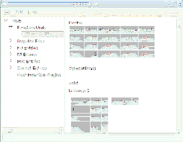
HDB Editor (hdbeditor) is a graphical frontend for creating and modifying Hardware Databases i.e. HDB files (see Section 2.2.3 for details). By default, all the example HDB files are stored in the directory hdb/ of the TCE installation directory.
This section is intended to familiarize the reader to basic usage of the HDB Editor.
HDB editor can be launched from command line by entering:
hdbeditor
You can also give a .hdb-file as parameter for the hdbeditor:
hdbeditor customHardware.hdb
Choose ``File'' | ``Create HDB...''. From there, type a name for your .hdb file and save it in the default HDB path (tce/hdb).
After that, you can start adding new TTA components such as function units, register files, buses and sockets from ``Edit'' | ``Add''.
The architecture implementation can be given either by hand or by a VHDL file.
After setting up the architecture, one can add new entries (function units, register files, buses, sockets) for the architectures.
To enable SRAM based register files in the implementation TCE must be notified if a implementation of RF requires separate address cycle. This is done in HDBEditor by setting option ``Separate address cycle'' to true in the Register File Implementation dialog. This option adjusts the timing of read accesses to be a cycle earlier. The option is effective only if default IC / Decoder Plugin (see: 4.5.1) is used to generate the machine since it does necessary modification to the instruction pipeline to tweak timings.
HDB includes a single SRAM register file implementation using dual-port block RAM inferred by Xilinx XST synthesis tool.